- Home
- Services
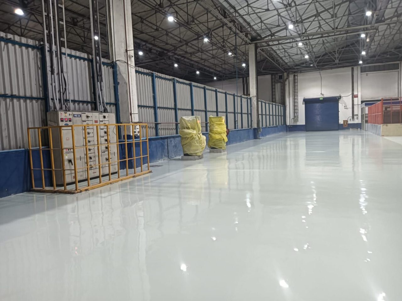
- EPOXY FLOORING
- POLYURETHANE FLOORING
- DI-ELECRIC FLOORING
- ANTI-STATIC EPOXY FLOORING
- ESD FLOORING
- ACCESS FLOORS
- CAR PARK DECK FLOORING
- CLEAN ROOM FLOORING
- HEAVY DUTY EPOXY FLOORING
- HYGIENE FLOORING
- SELF LEVELLING EPOXY FLOORING
- COLD STORAGE FLOORING
- ACID RESISTANCE FLOORING
- CAR PARK COATING
- EXPANSION JOINTS
- Projects
- Blog
- About Us
- Contact
Fundamentals of ESD: Part 1
To many people, Electrostatic Discharge (ESD) is only experienced as a shock when touching a metal doorknob after walking across a carpeted floor or after sliding across a car seat. However, static electricity and ESD has been a serious industrial problem for centuries. As early as the 1400s, European and Caribbean military forts were using static control procedures and devices trying to prevent inadvertent electrostatic discharge ignition of gunpowder stores.
Today, ESD impacts productivity and product reliability in virtually every aspect of the global electronics environment.
Despite a great deal of effort during the past thirty years, ESD still affects production yields, manufacturing cost, product quality, product reliability, and profitability. The cost of damaged devices themselves ranges from only a few cents for a simple diode to thousands of dollars for complex integrated circuits. When associated costs of repair and rework, shipping, labor, and overhead are included, clearly the opportunities exist for significant improvements. Nearly all of the thousands of companies involved in electronics manufacturing today pay attention to the basic, industry accepted elements of static control. ESD Association industry standards are available today to guide manufacturers in establishing the fundamental static charge mitigation and control techniques (see Part Six – ESD Standards). It is unlikely that any company which ignores static control will be able to successfully manufacture and deliver undamaged electronic parts.
Static Electricity: Creating Charge
Definitions for Electrostatic Discharge Terminology are in the ESD ADV1.0 Glossary which is available as a complimentary download at www.ESDA.org.
Electrostatic charge is defined as “electric charge at rest”. Static electricity is an imbalance of electrical charges within or on the surface of a material. This imbalance of electrons produces an electric field that can be measured and that can influence other objects.
Electrostatic discharge (ESD) is defined as “the rapid, spontaneous transfer of electrostatic charge induced by a high electrostatic field. Note: Usually, the charge flows through a spark between two bodies at different electrostatic potentials as they approach one another”.
Electrostatic discharge can change the electrical characteristics of a semiconductor device, degrading or destroying it. Electrostatic discharge also may upset the normal operation of an electronic system, causing equipment malfunction or failure. Charged surfaces can attract and hold contaminants, making removal of the particles difficult. When attracted to the surface of a silicon wafer or a device’s electrical circuitry, air-borne particulates can cause random wafer defects and reduce product yields.
Controlling electrostatic discharge begins with understanding how electrostatic charge occurs in the first place. Electrostatic charge is most commonly created by the contact and separation of two materials. The materials may be similar or dissimilar although dissimilar materials tend to liberate higher levels of static charge. For example, a person walking across the floor generates static electricity as shoe soles contact and then separate from the floor surface. An electronic device sliding into or out of a bag, magazine or tube generates an electrostatic charge as the device’s housing and metal leads make multiple contacts and separations with the surface of the container. While the magnitude of electrostatic charge may be different in these examples, static electricity is indeed formed in each case.
Creating electrostatic charge by contact and separation of materials is known as “triboelectric charging.” The word “triboelectric” comes from the Greek words, tribo – meaning “to rub” and elektros – meaning “amber” (fossilized resin from prehistoric trees). It involves the transfer of electrons between materials. The atoms of a material with no static charge have an equal number of positive (+) protons in their nucleus and negative (-) electrons orbiting the nucleus. In Figure 1, Material “A” consists of atoms with equal numbers of protons and electrons. Material B also consists of atoms with equal (though perhaps different) numbers of protons and electrons. Both materials are electrically neutral.
Have Any Question?
- +91 9962699888
- Sales@Chemcoats.com
- 19/10, Rangarajapuram 3rd Street, Netaji Nagar, West Jafferkhanpet, Chennai, Tamil Nadu 600083
- Sales@Chemcoats.com
- +91 9962699888